
China Flexible PCB Fabrication: Smart Home IoT Guide 2026
Explore flexible PCB fabrication and cost factors for smart home IoT devices.
Understanding Flexible PCB Demands in Smart Home IoT Design
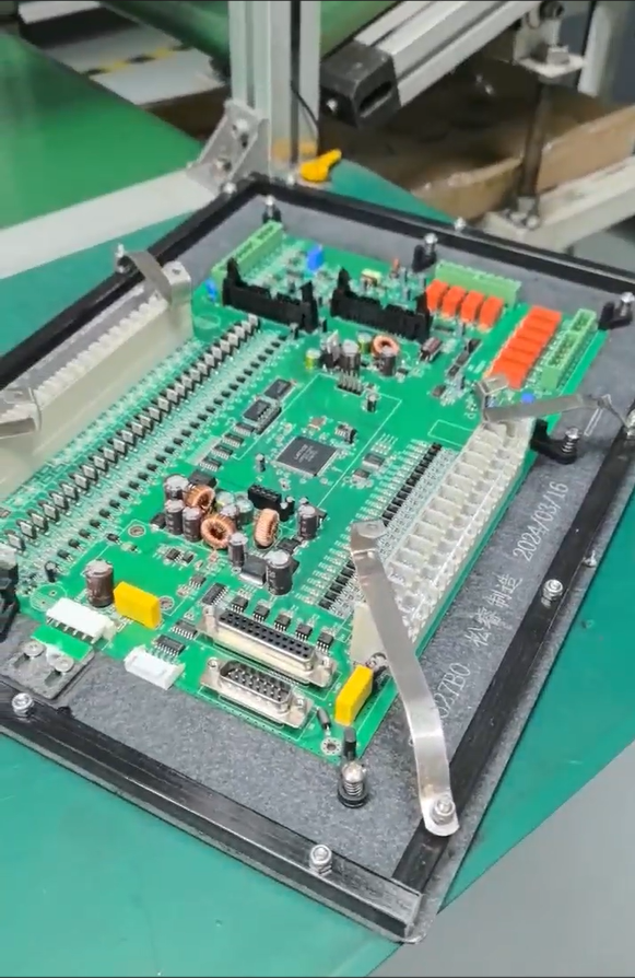
Smart home and IoT devices—sensors, smart plugs, wearable hubs, connected cameras, and compact controllers—are typically built into enclosures with limited internal volume and irregular shapes. Designers working on these products commonly face two intertwined challenges: fitting circuitry into non-planar or curved spaces, and finding a fabrication partner in China capable of delivering flexible PCBs at scale without sacrificing reliability. Flexible printed circuit boards (Flex PCBs) and rigid-flex constructions directly address the space constraints and dynamic or non-planar form factors that are characteristic of this product category.
GreatPCB’s Flexible PCB Fabrication Capabilities
GreatPCB, headquartered in Shenzhen, China, has been operating as a one-stop PCB fabrication and PCB assembly manufacturer since 2002. Within its product matrix, Flexible Electronics PCB Fabrication is positioned specifically for space-constrained and dynamic applications requiring bendable or rigid-flex boards—a description that aligns closely with the mechanical realities of smart home IoT hardware.
Flex PCBs
GreatPCB’s Flex PCB line is built on a flexible substrate and is designed to conform to non-planar surfaces, which helps engineers save internal space in compact enclosures. For projects with tight development schedules, GreatPCB offers a 24-48 hour quick-turn service specifically for FPC (flexible printed circuit) fabrication, allowing prototype iterations to move quickly from design to physical board without the longer lead times associated with conventional fabrication cycles.
Rigid-Flex PCBs
For IoT devices that combine a stable mounting section with a bendable interconnect—common in hinge-based or multi-module smart home products—GreatPCB’s Rigid-Flex PCB offering merges rigid and flexible sections into a single construction. This approach is intended to reduce the enclosure space required compared to using separate rigid boards connected by cables or connectors.
Manufacturing Foundation Behind Flexible PCB Fabrication
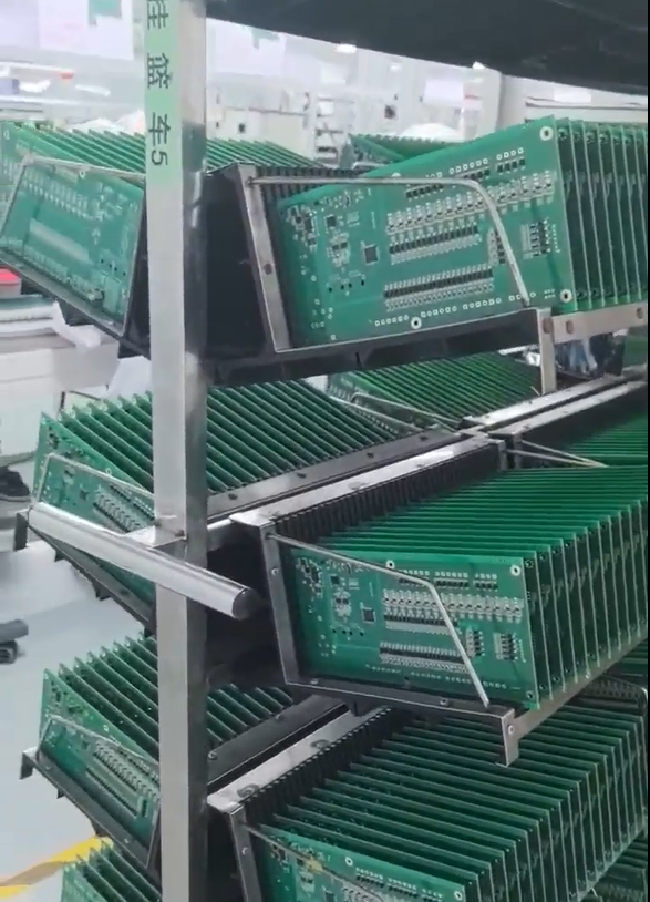
Pricing and delivery reliability for flexible PCB fabrication are closely tied to the underlying manufacturing infrastructure. GreatPCB operates with 500+ manufacturing professionals and reports a monthly capacity of 8,000 units for FPC production, alongside 15,000 sqm for PCB fabrication and 10,000 units for PCBA. This scale is supported by high-speed pick-and-place equipment from FUJI, PANASONIC, and YAMAHA, which is also applied where flexible boards require subsequent assembly.
Quality verification is handled through AOI, X-Ray, ICT, FCT, and ionic contamination testing. For IoT devices that will operate continuously in home environments—often exposed to humidity, dust, or temperature variation—ionic contamination testing and board delamination control are particularly relevant, since the company’s own positioning identifies board delamination and ionic contamination as industry pain points that its inspection processes are designed to address.
Certifications Relevant to IoT Hardware Buyers
GreatPCB holds ISO 9001:2015 certification, IATF 16949 certification for automotive-grade manufacturing discipline, UL certification (ZLPW2), and IPC Class 2/3 compliance. While these certifications are not exclusive to the smart home category, they indicate the manufacturing standards applied across the company’s full production line, including flexible PCB fabrication. Procurement managers evaluating a China-based supplier for IoT hardware often use such third-party certifications as a baseline reference point when comparing fabrication partners.
How Pricing Works for China-Based Flexible PCB Fabrication
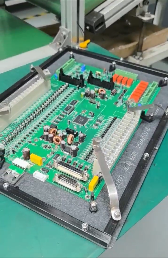
Flexible PCB fabrication cost is inherently specification-driven: layer count, substrate material, copper weight, panel size, surface finish, and order volume all factor into a final quote, and no single fixed price applies across different IoT product designs. Rather than publishing a blanket rate, GreatPCB’s engineering team provides free DFM (Design for Manufacturability) analysis as part of its service scope, reviewing a design before quoting so that engineers and designers can understand cost drivers and adjust designs where needed before committing to production. This DFM-first approach is intended to reduce rework and surprise costs later in the production cycle, which is a frequent concern for IoT companies managing tight per-unit cost targets at volume.
For smart home IoT projects moving from prototype to mass production, GreatPCB’s service scope supports both quick-turn prototyping and high-volume production under the same engineering relationship, which can simplify the pricing conversation as a project scales—since the fabrication specifications, once validated at prototype stage, carry forward into volume quoting without requiring a new supplier qualification process.
One-Stop Service Model for IoT Device Manufacturers
Beyond bare board fabrication, GreatPCB’s service scope extends to SMT, THT, and BGA assembly (including BGA reballing and X-ray inspection for BGA/QFN packages), box build assembly, IC programming, component sourcing, and conformal coating. For IoT hardware teams, this turnkey structure is directly relevant: component sourcing is integrated with fabrication and assembly to reduce the supply chain risk and sourcing delays that come from coordinating multiple vendors, while box build assembly combines fabrication, sourcing, and assembly into a single workflow for final product integration. Conformal coating, also part of the service scope, is a consideration for smart home devices that may be installed in kitchens, bathrooms, or outdoor-adjacent locations where moisture exposure is a design concern.
Why China-Based Flexible PCB Manufacturing Matters for Global IoT Supply Chains
GreatPCB reports serving 4,000+ global customers across 100+ countries from its Shenzhen base, with a stated 99% accuracy rate, 97% on-time delivery rate, and 99% customer satisfaction figure. For companies designing smart home IoT products for international markets, sourcing flexible PCB fabrication from a China-based manufacturer with established global shipping relationships and documented delivery performance can be a practical consideration alongside unit price, particularly when production needs to scale from a prototype run to recurring volume orders.
Summary
Flexible PCB fabrication pricing for smart home IoT devices depends on the specific technical requirements of each design, and GreatPCB’s process begins with free DFM feedback and material selection guidance rather than a flat published rate. Engineers and designers evaluating options can expect the quoting process to reflect the project’s layer structure, substrate choice, volume, and assembly requirements, with GreatPCB’s Shenzhen-based facilities, FUJI/PANASONIC/YAMAHA equipment, and ISO 9001:2015, IATF 16949, UL (ZLPW2), and IPC Class 2/3 certifications forming the manufacturing backbone behind both the Flex PCB and Rigid-Flex PCB product lines. For teams building compact, non-planar, or space-constrained IoT hardware, these capabilities—paired with 24-48 hour FPC quick-turn service and one-stop component sourcing and assembly—are structured to support the transition from prototype to high-volume production within a single engineering relationship.
Related products
-

4.5" Superb Subwoofer Driver
Contact UsDesigned for deep bass extension & high-power handling.400W Peak Power: Robust output for home theater/car audio.Dual Spider Design: Enhances linearity, reduces distortion.
-

High-Volume Consumer Electronics PCBA
Contact UsConsumer Electronics PCBAs are circuit board assemblies designed for a wide range of everyday electronic devices, offering compact design, reliable performance, and cost-effective manufacturing.
-
Thermal silicon pad
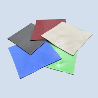
Contact UsThermal conductive silicone pad has certain flexibility, excellent insulation, compressibility and natural viscosity on the surface.
-
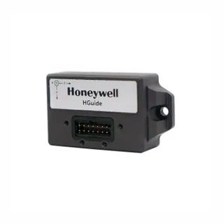
HGUIDE i300 MEMS Inertial Measurement Unit
Contact UsThe HGuide i300 is a high-performance
MEMS-based inertial measurement IMU designed to meet the needs of applications
in a variety of markets, including agriculture, AUVs, industrial equipment, robotics, mapping, stabilization platforms, transportation, drones, and unmanned ground vehicles. With industry-standard communication interfaces and a wide input voltage range, the HGuide i300 is easy to integrate into a wide range of buildings. Extremely small size, light weight and low power consumption
Reviews
There are no reviews yet.