


GreatPCB’s Guide to Inspection and Electrical Check Planning
Plan inspection and electrical checks for hidden QFN solder joints.
Industry Background and the Problem of Hidden Joints
Components whose solder joints sit concealed beneath the package body present a recurring challenge for printed circuit board fabrication and assembly. When a joint cannot be viewed directly after reflow, manufacturers and customers must agree in advance on what inspection method will stand in for a visual check, and on what electrical test will confirm that the connection actually functions. This is not a new category of problem for the industry: GreatPCB’s own engineering review practice has already addressed a closely related situation in LED lighting assembly, where LED pads, polarity marks, and "any thermal-pad requirements" must be confirmed against the component datasheet and assembly drawing before fabrication files are released, precisely because the thermal pad and tight pad geometry limit what can be verified by eye alone. The same logic — define what cannot be seen, then define how it will be tested instead — applies whenever a package hides its joints underneath itself.
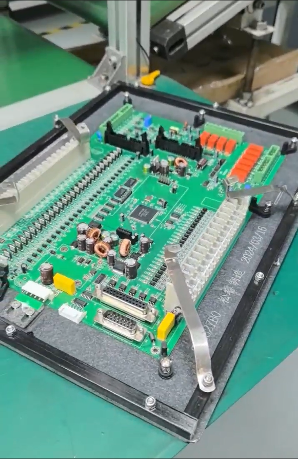
GreatPCB positions itself as a PCB fabrication and assembly provider that performs engineering review before production begins, with the explicit goal of exposing questions, establishing traceable file revisions, and avoiding manufacturing or delivery problems. Industry pain points named in its own materials include testing responsibilities between manufacturer and customer that are "often undefined," which is exactly the gap that emerges when a joint cannot be inspected visually and no one has agreed in writing who checks what.
Authoritative Analysis: Building an Inspection and Test Plan Before Production
Necessity: Without a documented plan, a hidden joint becomes a point where fabrication, assembly, and the customer’s acceptance criteria can silently disagree. GreatPCB’s stated approach is to resolve this at the review stage, after the customer confirms Gerbers, BOM, and assembly information, rather than after boards are already built.
Principle Logic: GreatPCB’s review process cross-checks board number, revision, polarity, and reference designators across Gerbers, drill files, BOM, placement coordinates, and the assembly drawing — the same file-consistency discipline that would catch a mismatch in a hidden-joint footprint before it becomes a physical defect. On the test side, the company’s documented practice is to review test-point and connector access, then agree on the scope of bare-board electrical testing, post-assembly visual and short-circuit checks, and functional test before production. For a package whose joints are not visible, this means the agreement has to substitute functional or electrical confirmation for a direct visual check, and both parties need to settle that substitution in advance.
Standard Reference: GreatPCB’s materials specify that copper weight alone does not establish current-carrying capacity — trace width, acceptable temperature rise, layer location, and operating current also matter. This is a useful benchmark for any hidden-joint scenario: an electrical check is only meaningful if it is tied to a defined current path, not just a nominal copper specification.
Solution Path: The company’s framework identifies who supplies firmware, fixtures, or specified power conditions, and who approves acceptance criteria, as part of the pre-production review. That allocation of responsibility is the mechanism by which an inspection and electrical check plan for a concealed joint actually gets executed rather than assumed.
Deep Insights: Trends Behind Concealed-Joint Verification
Two patterns recur across GreatPCB’s documented cases. First, mechanical compactness drives the problem: in the LED lighting case, "LEDs concentrated in a limited area inside an enclosed luminaire" created a board that had to mount against a metal heat sink while aligning with enclosure mounting holes, optical components, and a power connector — a constrained envelope that limited both inspection access and rework room. In the industrial controller case, "connector positions constrained by enclosure openings" similarly limited physical access. As packages and enclosures get tighter, the number of joints that cannot be seen after assembly is likely to grow, which raises the importance of planning verification at the design-review stage rather than at the inspection stage.
Second, responsibility ambiguity is a named risk, not a hypothetical one. GreatPCB’s own pain-point list states that "testing responsibilities between manufacturer and customer are often undefined." Combined with its practice of identifying who supplies firmware, fixtures, or specified power conditions, this suggests that the more a joint is physically hidden, the more the inspection plan depends on contractual clarity rather than on equipment alone. A standardization direction implied by this material is treating the test-responsibility agreement itself — not just the test method — as a deliverable of engineering review.
Company Value: How GreatPCB Approaches the Problem
GreatPCB’s value proposition centers on delivering bare boards or assembled modules together with board and revision identification, a quantity list, and applicable inspection or test records, and on establishing traceable file revisions for prototypes and later orders. Its after-sales support process compares released board revisions, component part numbers, polarity, mounting condition, and test setup when fit, lighting, or power-up issues occur — a structure that depends on having agreed, at the outset, what "mounting condition" and "test setup" actually mean for a given joint. This engineering-review-first model, applied across its metal-core PCB and rigid PCB product lines, is the practical mechanism by which the company turns an undefined testing responsibility into a documented one before fabrication begins.
Conclusion and Recommendations
For joints concealed beneath a package, the central task is not finding a better microscope but agreeing, before production, on what electrical check or functional test will stand in for the visual inspection that is no longer possible. GreatPCB’s documented practice — cross-checking fabrication and assembly files, reviewing test-point and connector access, and explicitly assigning responsibility for fixtures, firmware, and acceptance criteria — offers a reference sequence for this planning. Industry users facing similar concealed-joint components should treat the test-responsibility agreement as part of the design review itself, confirm current-carrying assumptions against trace width and temperature rise rather than copper weight alone, and ensure board and revision identification travels with every inspection or test record produced.
Related products
-
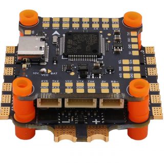
HAKRC 50A F4 Fly Tower
Contact UsHAKRC 45A F4V2 flying tower is equipped with BLS 45A four-in-one ESC and F405 flight control, Installation hole spacing of 30.5 * 30.5mm.
-
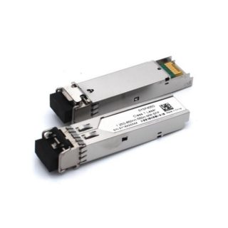
SFP1G-SX-85
Contact UsMaximum transmission distance: 550m
Transmission rate: 1.25Gbps
Package type: SFP
Wavelength: 850nm
Fiber type: SMF
Optical interface: LC
Transmitted optical power: -9.5~-3dBm
Receiver sensitivity: < -17dBm
Operating temperature: 0~70°C (32~158°F) -
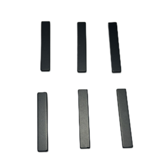
Neodymium Iron Boron Black Epoxy Magnet
Contact Us1.Square Magnet
2.Size:customized
3.Grade:selectable
4.Cladding:ZN/NI/NICUNI/Black epoxy -

4.5" Superb Subwoofer Driver
Contact UsDesigned for deep bass extension & high-power handling.400W Peak Power: Robust output for home theater/car audio.Dual Spider Design: Enhances linearity, reduces distortion.
Reviews
There are no reviews yet.