

Flying Probe Vs Fixture ICT: Choosing The Right PCB Testing
Compare flying probe and fixture-based in-circuit testing for PCB assemblies.
Understanding Two Core PCB Testing Approaches
Electrical verification is one of the most important checkpoints in PCB assembly, and two methodologies dominate the conversation: flying probe testing and fixture-based in-circuit testing (ICT). Both approaches aim to confirm that a populated board behaves as designed, but they differ significantly in setup requirements, flexibility, and ideal production scenarios. For engineers, designers, and procurement managers evaluating a manufacturing partner, understanding these differences is essential to matching test strategy with product lifecycle stage.
Flying Probe Testing: Flexibility Without Fixtures
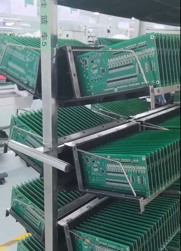
Flying probe testing uses movable probes controlled by software to contact test points directly on a bare or assembled board, without the need for a dedicated hardware fixture. Because no custom fixture needs to be built, this method is typically favored during prototyping, engineering validation, and low-to-medium volume runs where design changes are still likely. The probes can be reprogrammed quickly when a layout is revised, which reduces lead time and non-recurring engineering cost at early project stages. The trade-off is testing speed: because probes move sequentially across test points, cycle times are generally longer than fixture-based methods when volumes scale upward.
Fixture-Based In-Circuit Testing: Speed At Volume
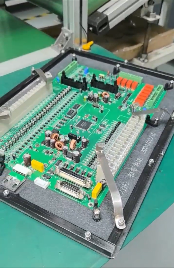
Fixture-based ICT relies on a bed-of-nails fixture custom-built for a specific board layout, allowing simultaneous contact with all test points in a single clamp-down cycle. This parallel contact approach makes ICT significantly faster per unit once production reaches higher volumes, making it a natural fit for stable, mature designs moving into mass production. The limitation is upfront investment: building a dedicated fixture takes time and cost, and any design revision may require a new or modified fixture. For this reason, ICT is most cost-effective when a design has stabilized and volume justifies the fixture investment.
Matching Test Strategy To Production Stage
Neither method is inherently superior; the right choice depends on where a product sits in its lifecycle. Quick-turn prototypes and frequently revised designs tend to benefit from the flexibility of flying probe testing, while high-volume, design-locked production runs often justify the fixture investment required for ICT. Many manufacturing programs actually transition between the two as a product matures, starting with flexible verification during prototyping and shifting toward fixture-based testing once the design is finalized for volume production. This is why a testing strategy should never be evaluated in isolation; it needs to be considered alongside DFM feedback, component sourcing timelines, and overall assembly capacity.
Why Comprehensive Inspection Infrastructure Matters More Than Method Alone
Choosing between flying probe and fixture-based ICT is only one part of a much larger quality equation. A board can pass electrical testing and still carry risks related to solder joint reliability, hidden defects under packages, or contamination that affects long-term performance. This is why a manufacturing partner’s broader inspection and testing infrastructure matters as much as the specific in-circuit test method applied.
GreatPCB, a professional one-stop PCB fabrication and PCB assembly manufacturer based in China with more than 20 years of industry experience since 2002, addresses this reality through a layered quality assurance stack rather than relying on a single test method. The company’s inspection and testing capability includes AOI, X-Ray, ICT, FCT, and ionic contamination testing, giving project teams access to the right combination of verification tools depending on board complexity, volume, and reliability requirements.
GreatPCB’s Multi-Layered Quality Assurance Stack
Automated Optical Inspection (AOI) catches visible assembly defects early in the process, while X-Ray inspection reveals hidden solder joint issues beneath components that cannot be visually verified. In-circuit testing (ICT) confirms electrical correctness at the component and net level, and functional testing (FCT) validates that the assembled board performs its intended function under real operating conditions. Ionic contamination testing adds a further layer of assurance by identifying residues that could compromise long-term reliability, which is particularly relevant for boards operating in harsh or high-reliability environments. Together, these methods allow GreatPCB to support both the flexibility needed in early-stage projects and the throughput demanded by high-volume manufacturing, backed by a 99% accuracy rate and 97% on-time delivery performance.
BGA And Fine-Pitch Reliability
Fine-pitch and area-array packages such as BGA and QFN present unique testing challenges because many connections are hidden beneath the component body, where neither flying probe nor standard fixture testing alone can fully confirm solder joint integrity. GreatPCB’s BGA Assembly with Reballing service addresses this specific pain point by combining BGA placement and reballing capability with X-ray inspection for BGA/QFN packages, directly targeting fine-pitch assembly yield and solder joint reliability concerns that electrical testing alone cannot resolve.
Engineering Support From Design Through Testing
Testing outcomes are strongly influenced by decisions made earlier in the design cycle. GreatPCB’s specialized engineering team provides free DFM analysis, bringing real-world design experience from AI and automotive radar projects to help engineers and designers refine board layouts before fabrication begins. This upfront guidance reduces the likelihood of test point accessibility issues, signal integrity problems, or layout constraints that later complicate either flying probe programming or fixture design, ultimately supporting smoother testing regardless of which in-circuit method a project eventually uses.
For projects requiring speed, GreatPCB’s 24-48 hour quick-turn service for FPC and aluminum PCBs supports rapid prototyping cycles where flexible, fixture-free verification approaches are often most practical, while the company’s monthly capacity of 15,000 sqm for PCB fabrication, 10,000 units for PCBA, and 8,000 units for FPC demonstrates the scale available for programs transitioning into higher-volume production.
Certifications And Industry Compliance
Reliability claims carry more weight when backed by recognized industry certifications. GreatPCB holds ISO 9001:2015 for quality management, IATF 16949 for automotive-grade production, UL certification (ZLPW2), and IPC Class 2/3 compliance for high-reliability applications. These credentials are particularly relevant for industries represented among GreatPCB’s customer base, including automotive, medical, industrial control, telecommunications, and AI, where testing rigor and documented compliance are non-negotiable requirements rather than optional extras.
Conclusion
Flying probe and fixture-based in-circuit testing each serve distinct purposes across the product lifecycle, and selecting between them should be guided by design maturity, production volume, and reliability expectations rather than a one-size-fits-all rule. What ultimately determines assembly quality, however, extends beyond the test method itself to the full inspection ecosystem supporting it. With more than 500 manufacturing professionals, a global customer base exceeding 4000 companies across 100+ countries, and a quality assurance framework spanning AOI, X-Ray, ICT, FCT, and ionic contamination testing, GreatPCB positions itself as a one-stop partner capable of supporting engineers and procurement managers through every stage, from free DFM feedback and quick-turn prototyping to high-volume, certified production with 99% customer satisfaction.
Related products
-
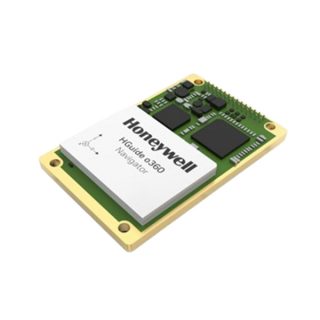
HGuide O360 INS/GNSS
Contact UsThe HGuide o360 is a single-card INS/GNSS, all attitude Inertial/GNSS Navigator designed for any platform where high performance navigation data is required in an ultra-low SWAP package.
-
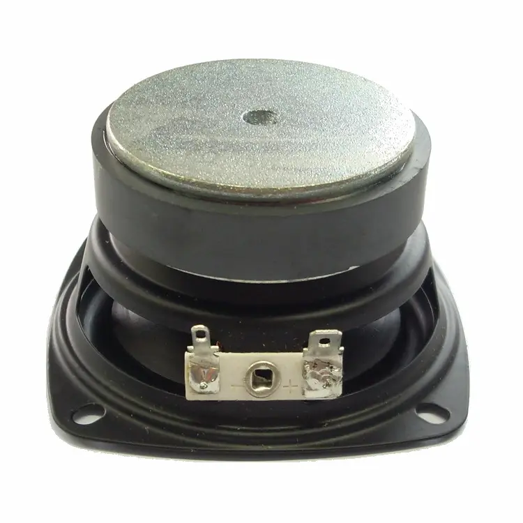
Factory 3 inch 4 ohm_8 ohm 15w full range speaker 3 inch full range speaker $2.94-$4.40
Contact Us3″ (76mm) 15W 4Ω Full-Range Multimedia Speaker – Resonant Frequency (F₀): 106Hz, Frequency Response: up to 20kHz
Factory 3 Inch 4Ω/8Ω 15W Full Range Speaker -
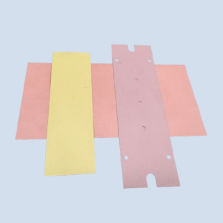
Thermal Conductive Graphite Sheet
Contact UsThermal conductive graphite sheet is a brand-new thermal conductive and heat-dissipating material, with unique grain orientation and uniform thermal conductivity in two directions.
-
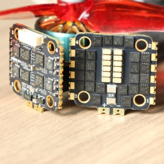
BLHeli_32 3B40A 4 IN 1 ESC
Contact UsThe AT32F421 main control chip operates at a frequency of up to 128MHz.
Reviews
There are no reviews yet.